Diagramming Microchips (McCarty 1990)
Cara McCarty's essay Information Art: Diagramming Microchips in on moma.com.updates
wait, they're actually colored like that?
introduction
to link it to the wealth of additional material since been made available online.
Since the end of World War II developments in technology have produced objects, seldom seen by the public, very different in appearance from the geometric shapes that have so far characterized Machine Art. The growing complexity of our machines has led to the miniaturization of parts; electronics has altered out conception of how things need to be shaped in order to work, and of how they must be related to each other.
The new machine art is visually incomprehensible unless one knows about and believes in the existence of invisible forces. Geometric machine art suggested by its finite shapes the direct action of push and pull: the new machines, or parts of machines, consist often of patterns. Printed circuits in particular, and the use of wires colored for identification in the RAMAC control panel, suggest one change that technology is likely to make on many of our common artifacts: the dematerialization of solid forms into clusters of linear relationships.
Arthur Drexler
Twentieth Century Design from the Museum Collection
The Museum of Modern Art, 1958
diagrams
 Texas Instruments c. 1976
122 transistors
Logic Chip (experimental)
Texas Instruments c. 1976
122 transistors
Logic Chip (experimental)
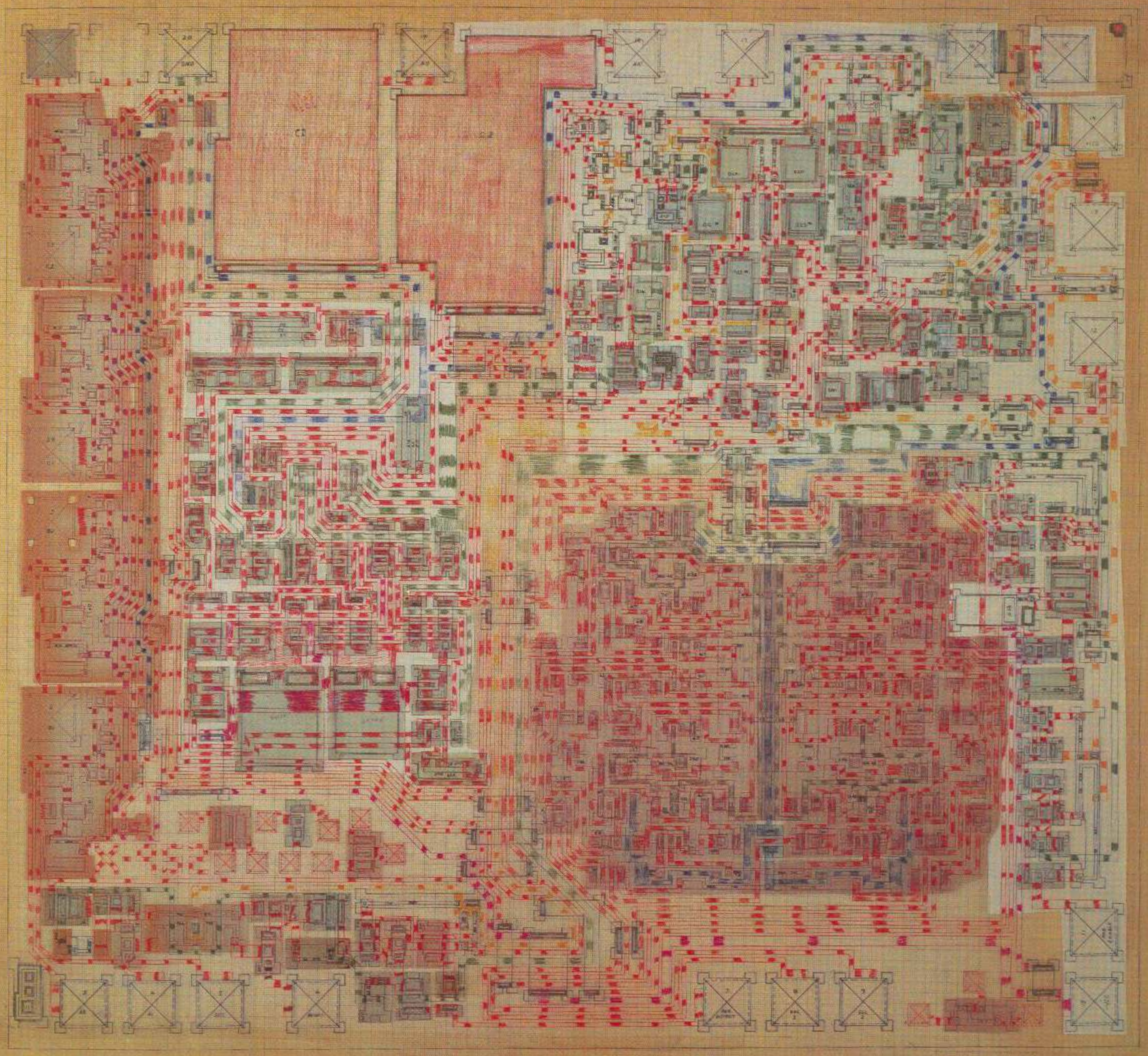
At the time this plot was hand drafted, it was still possible to verify the design of individual components visually. To repeat a circuit element multiple times, an engineer would trace the initial drawing of the component, photocopy it onto mylar, then cut and glue it onto the diagram. The collage technique is referred to as "paper-doll layout." Intended for use in a military computer, this particular chip was designed to sense low-level memory signals, amplify the signals to a specific size, and then store them in a memory cell for later recall.
 IBM, East Fishkill, New York
1986
15,000 transistors
Logic Chip
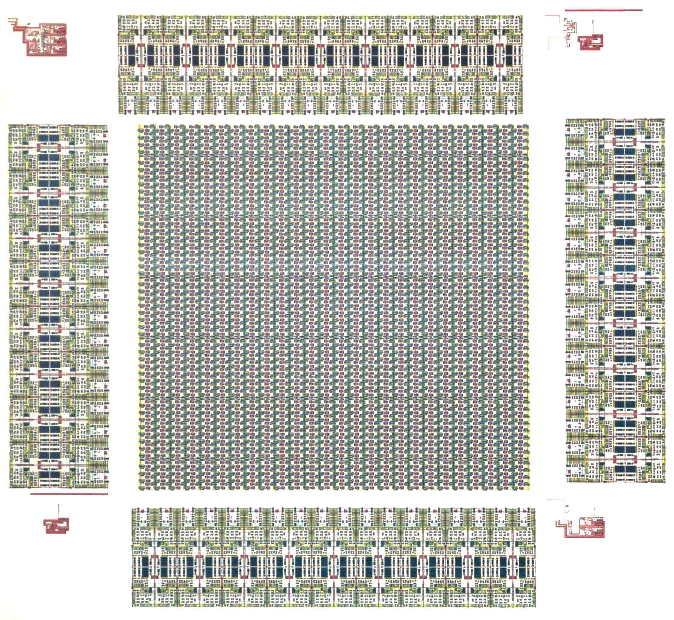
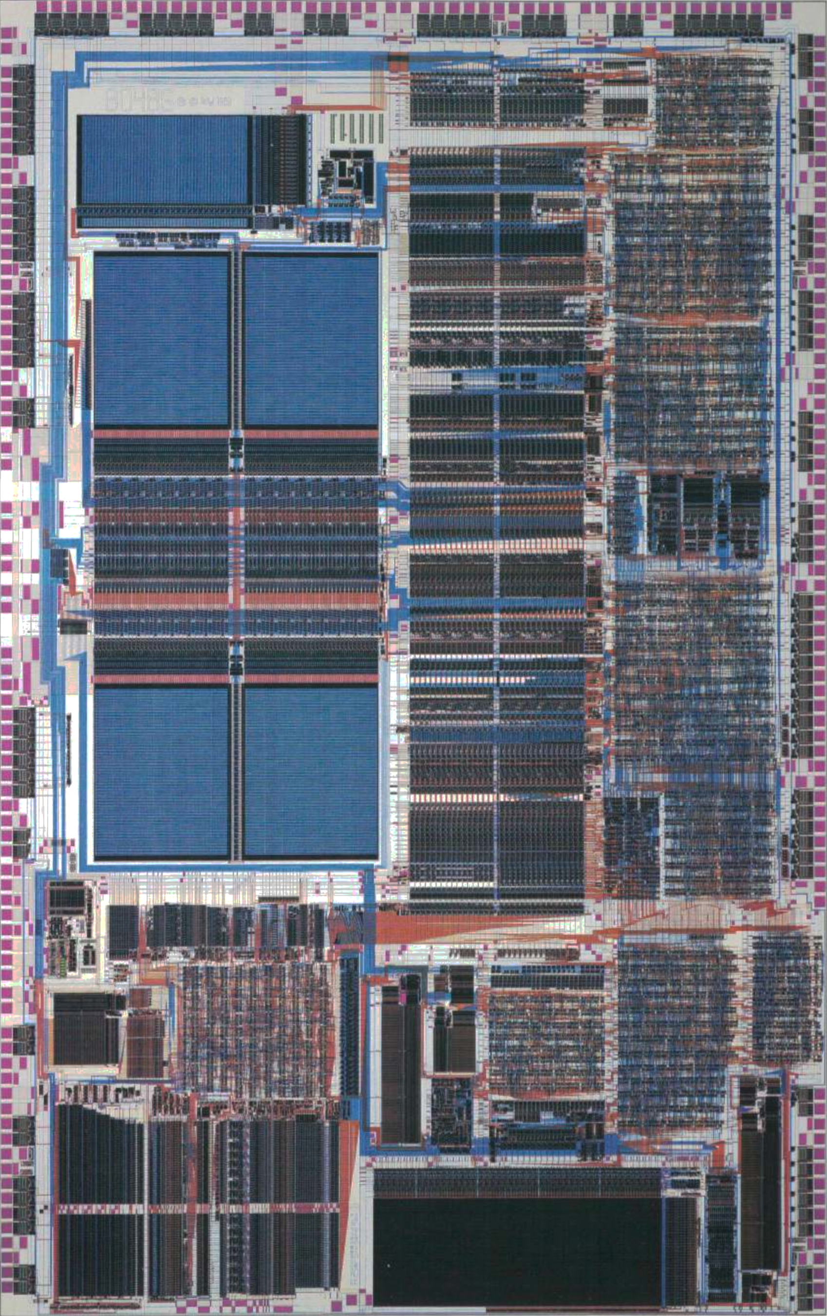
IBM, East Fishkill, New York
1986
15,000 transistors
Logic Chip
The devices on this chip are wired together to perform many different arithmetic and logic functions, and are used to assist a microprocesor in a personal computer. The uniform pattern is achieved, not with the collage technique of the previous diagram, but by using the computer to repeat one cell thousands of times. The diagram on the right shows the last metal layer that goes on top of the chip illustrated above. The orange and blue patterns represent wires that are used to distribute power to the components in the layers below.
memory
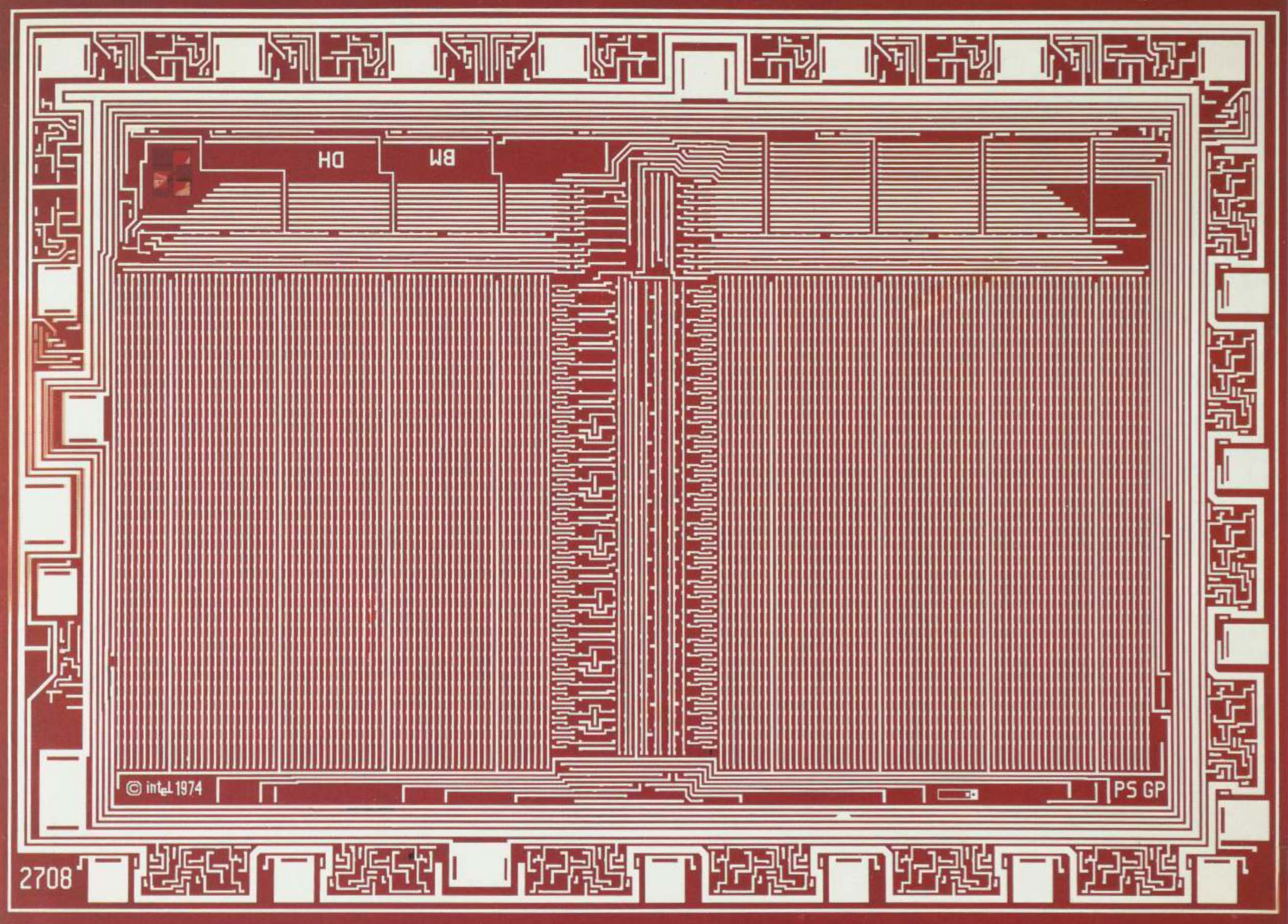 Intel Corporation
1974
Erasable Programmable Read-Only Memory Chip (EEPROM)
Intel Corporation
1974
Erasable Programmable Read-Only Memory Chip (EEPROM)
Before companies used computers to assist with the design of integrated circuits, the entire process of creating a chip was performed manually. After the design was hand drawn on paper, operators hand cut the circuit pattern into red cellophane-like sheets called rubylith. The design was then reproduced photographically. The diagram illustrated here represents the metal mask, the last significant layer in the fabrication process.IBM, Burlington, Vermont 1982 288,000 transistors Dynamic Random-Access Memory Chip (DRAM)
There are different types of memory chips, but the most common are known as DRAM. Often considered the main memory, they are the largest storage area within the computer. The termIBM, Burlington, Vermont 1984 1 million transistors Dynamic Random-Access Memory Chip (DRAM)random accessrefers to the ability to access the desired information directly, independently of other data in the storage unit. Unlike other memory chips, DRAMs store data and programs temporarily, only for as long as the power remains on.
Resembling a solid block, this dense and regular pattern is characteristic of memory devices. It has the capacity to store approximately one hundred pages of double-spaced typewritten text, or one-sixth of a 250-page paperback novel. Today's chips are capable of storing the equivalent of several novels.Texas Instruments 1985 over 1.2 million transistors Dynamic Random-Access Memory Chip (DRAM)
The data storage areas are located in the four uniform quadrants, and the intricate circuitry required to access the information is located at both ends of the device.
microprocessors
Digital Equipment Corporation 1975 8,000 transistors Central Processing Unit (microprocessor)TheIntel Corporation 1978 29,000 transistors Microprocessor (8086)brainof the computer itself is its central processing unit. Used primarily for medical purposes, this was the analytical element in an ultrasonic image-processor, which for example determines the status of a pregnancy without exposing the patient to potentially damaging X-rays. Other applications include those of controller for animated sign displays and remote processor for scientific experiments in hazardous areas.
The 8086 was developed for copiers, early robots, and numerous industrial applications, but its primary use is personal computers. Much of this diagram was designed by hand.Intel Corporation 1985 229,000 transistors Microprocessor (386__tm())
Microprocessors are the most varied pattern areas of all integrated circuits. Their web of circuitry is organized into distinct regions that perform a number of specialized functions. The diagrams on these two pages belong to the same family of microprocessors. The chip on the right is a more sophisticated and considerably faster version of the one above, accommodating what previously would have required five to six chips. The 386 chip serves many functions, and is found in trains, planes, laser printers, and telephone switches, but the most common use is in personal computers. The 486 microprocessor was designed to provide the computing power of a mainframe in a desktop computer. It is capable of executing over 20 million instructions per second.
 Intel Corporation
1989
1.2 million transistors
Microprocessor (486__tm())
Intel Corporation
1989
1.2 million transistors
Microprocessor (486__tm())
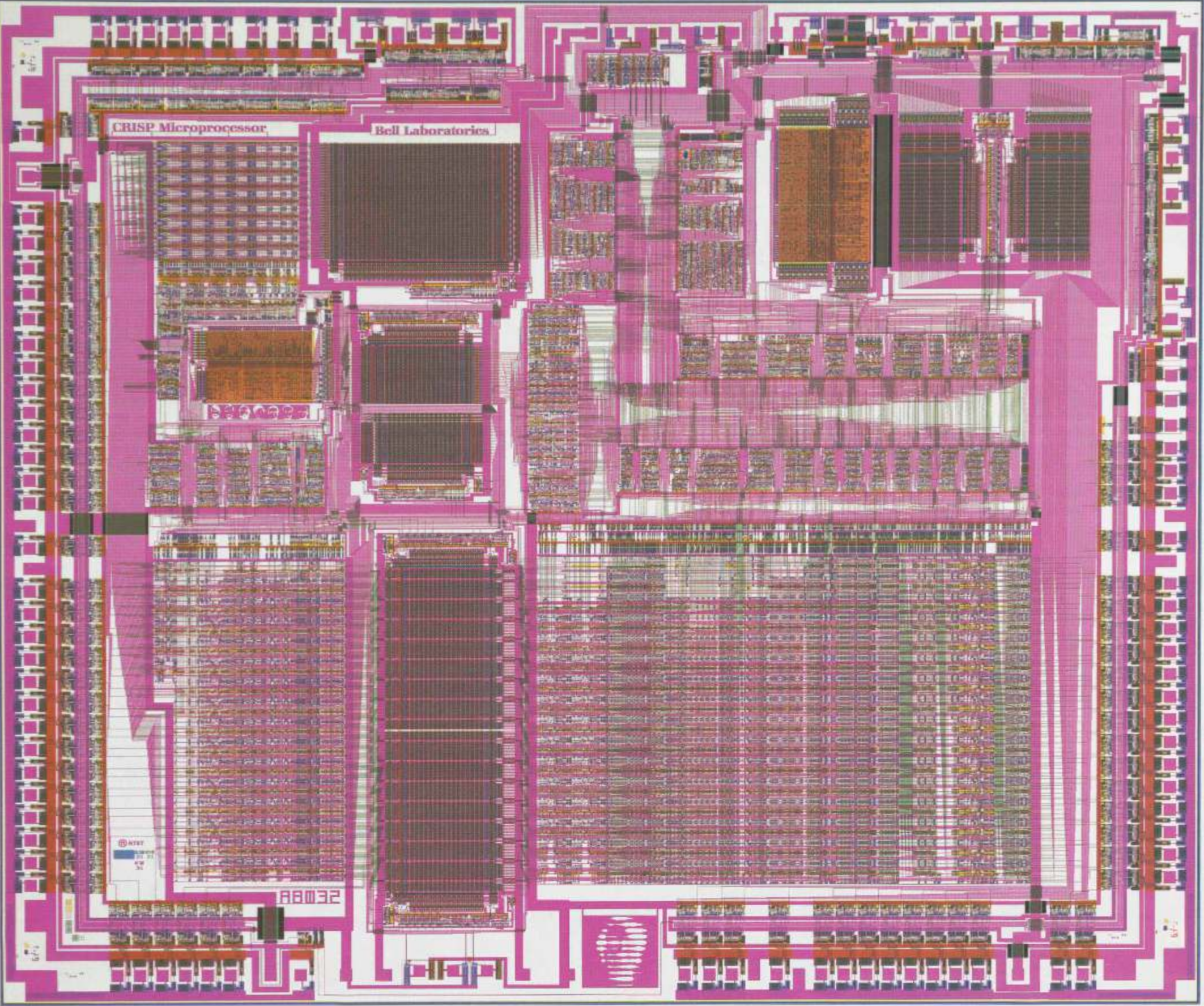 AT&T Bell Laboratories
1986
172,000 transistors
Microprocessor (CRISP)
AT&T Bell Laboratories
1986
172,000 transistors
Microprocessor (CRISP)
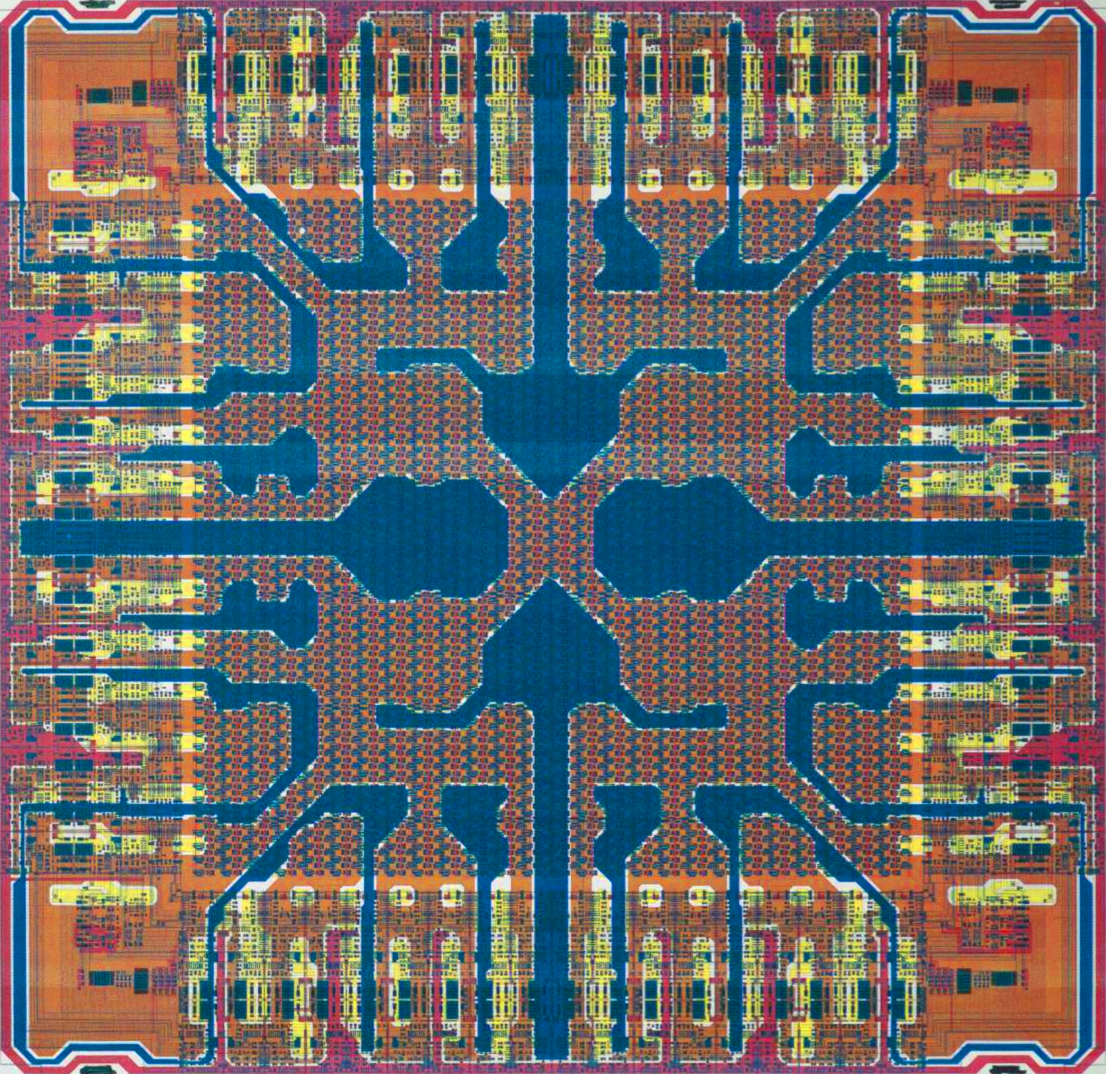
During the 1980s the field of computer architecture was revolutionized by the invention of the Reduced Instruction Set Computer (RISC processors). Prior to this machines were capable of performing hundreds of different basic operations, most of which were rarely used and introduced complications that limited computer speeds. By reducing the number of different instructions, designers were able to make each one quickly. Although more instructions were now needed to perform any given task, the net time to execute them declined. Because instructions were very simple, it became easier to pipeline them, that is, to execute several instructions simultaneously, assembly-line fashion. Moreover, the entire processor could be integrated into a single chip. The overall result was a dramatic increase in speed and reduction of cost. Opposite: four details showing circuit components at various levels of enlargement.
This is the heart of the central processing unit for a low-cost computer. It contains the computer's intellegence and control functions. The upper portion contains the logic sections, and the lower blocks are the memory files.
application specific
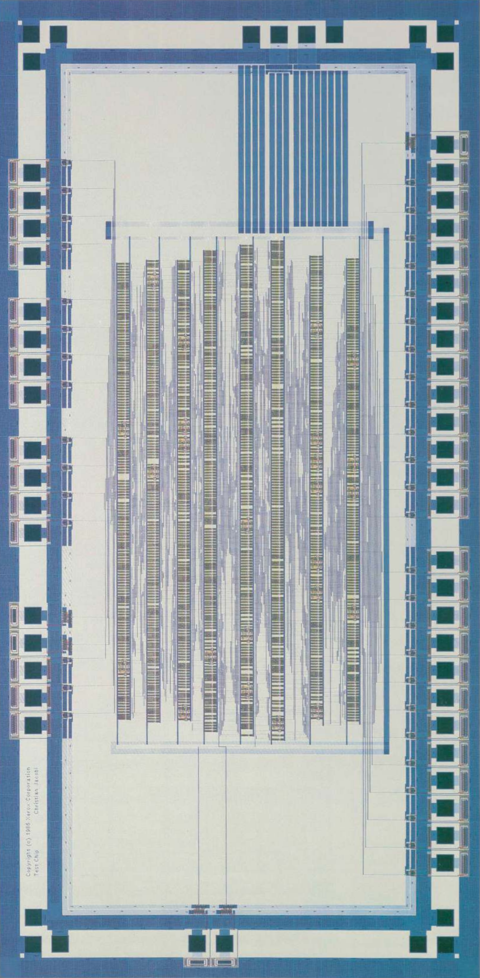 Xerox Alto Research Center
1986
approximately 3,000 transistors
Application Specific Integrated Circuit (ASIC), test chip
Xerox Alto Research Center
1986
approximately 3,000 transistors
Application Specific Integrated Circuit (ASIC), test chip
The diagram is of a chip used for testing components of a computer-aided design library.LSI Logic Corporation 1988 250,000 transistors Application-Specific Integrated Circuit (ASIC)
This was designed to improve image contrast in a variety of applications, including medical diagnosis, aerial reconnaissance, and automated inspection systems used in manufacturing. Developed as an application-specific product, it combines memory-cell and gate-array technologies in one chip. The details on the right are enlargements of the two main pattern areas. The top diagram shows the individual cells compromising the memory blocks, the bottom illustrates the gate arrays.VLSI Technologies Inc. 1986 33,500 transistors Application-Specific Integrated Circuits (ASIC)
This is an example of a gate array. It is a test chip used to verify the fabrication process and performance of chips. It has since been superceded by more sophisticated designs.
neural nets
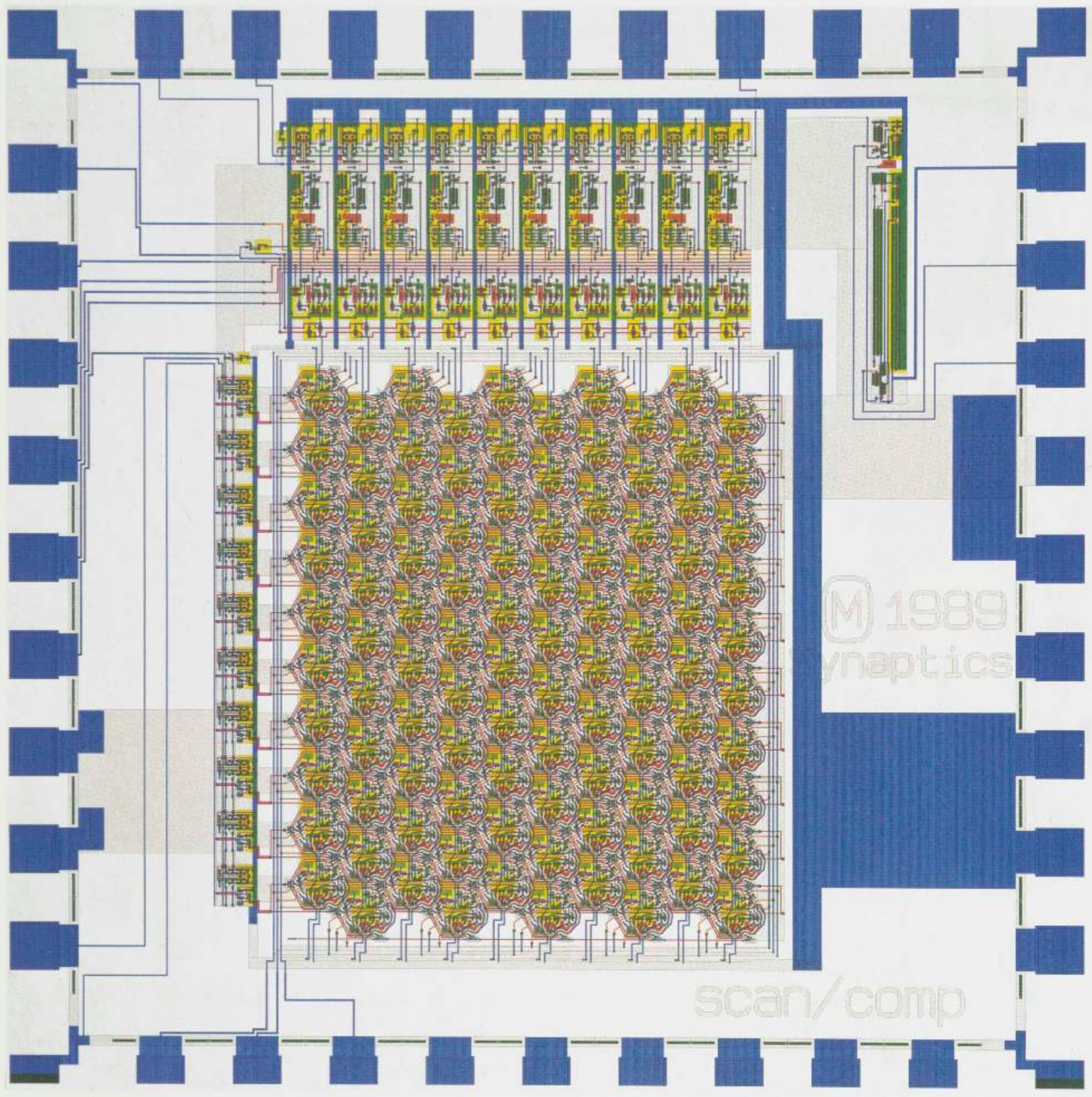 Synaptics, Inc.
1989
3,100 transistors
Neural Net (experimental)
Synaptics, Inc.
1989
3,100 transistors
Neural Net (experimental)
This chip is a photo sensor and was designed to mimic some of the functions of the human retina. Containing a core of 100 electronic processing cells that detect images when light strikes them, the chip performs two operations: it highlights detail in an image, and it orients and locates objects or other features by their edges. The information received by all the cells is averaged and then passed on to a computer for further inspection. The design is based on hexagonal-grid properties, as opposed to the rectangular- or square-grid format found in the other diagrams in this publication. With the hexagonal shape each cell is equidistant from its neighbors, which allows for smoother and more accurate gathering of data.
 IMEC and University of Pennsylvania
1989
Neural Net: foveated, retina-like sensor
IMEC and University of Pennsylvania
1989
Neural Net: foveated, retina-like sensor
The radial layout of this image sensor is loosely modeled on the human visual system, and consists of two parts: a peripheral and a central area (fovea). The outer part consists of 30 concentric circles and 64 sensors per circle whose size increases linearly with eccentricity. It is used for active vision, particularly in robots.